Custom RF/Analog IC Design
Circuit Design
Having worked primarily in startup environments, we have always been challenged for unconventional solutions to meet difficult specs and differentiate our ICs from the competition. In addition to this, yield, testability, volume manufacturability and time to market could not be neglected.
Our design capabilities include, but are not limited to:
- Chip ESD architectures and protection circuits
- Bandgaps, constant current and PTAT references
- Opamps, voltage references and general analog circuits
- Digital to analog converters
- Serial port interfaces
- Frequency synthesizers
- Programmable gain amplifiers
- RF transceiver blocks including:
- Mixers
- LNAs
- AGCs
- Filters
- Frequency Dividers/Doublers
- VCOs
Architectural Design
At the outset of a new transceiver design, a lead designer often does a rudimentary block and level analysis in parallel with their considerable design responsibilities. Alternatively, a systems group may scope out the transceiver architecture but often without doing any exploratory design work to determine feasible specs simply because transistor level design is not their core expertise.
This often results in a link budget that does not accurately reflect the system under development, makes gross assumptions about inter stage impedance levels and ultimately does not give accurate noise and linearity performance estimates. In either case, without a proper link budget analysis it is difficult to anticipate overall radio performance until finished silicon comes back and measurements are done. At that point, it can be very difficult to make any necessary changes without impacting schedule and constraints on all other blocks in the chain.
In all past transceiver designs we have always placed emphasis on having a relevant link budget analysis. 50 ohm I/O’s between blocks on chip are never assumed and as exploratory designs evolve, the link budget is updated to reflect new parameters. In some cases we have bridged the gap between systems groups and designers; and in other cases drafted out the architecture and link budget from scratch.
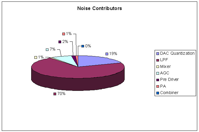
A section of a representative link budget gives the noise results shown below. With this, it becomes much easier to identify blocks that need improvement to yield the largest improvement in overall system performance.
PCB Design
As either a stand alone PCB design or a bench test card following first silicon design, all aspects of layout and coordination of board fabrication and population can be facilitated. Having core expertise in RF systems, a PCB layout with minimal iterations can be realized that ensures minimal impact of board parasitics on system performance. The PCB may also be handled in the context of a system on board design in which the system link budget, component selection and simulation is done.
Passive Device Modeling
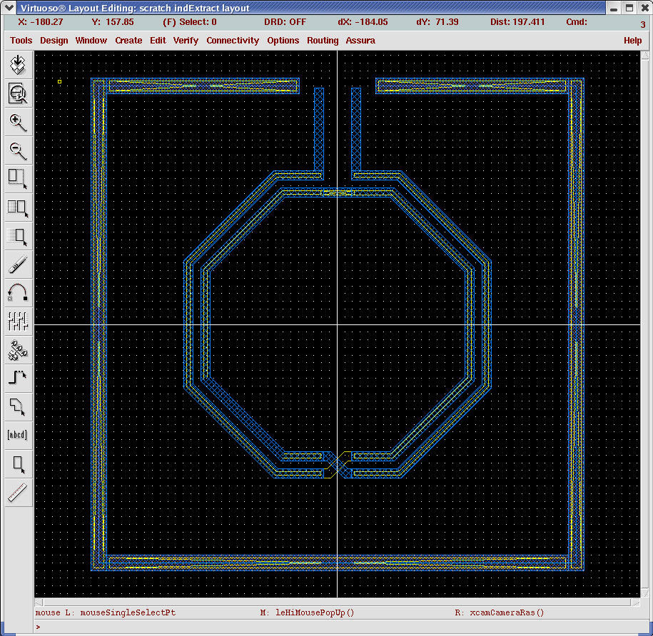
Design kits provided by most foundries contain only a limited selection of inductors and transformers. Designers frequently require more intricate passive structures or need to use foundry models at frequencies outside of their modeled range. Ground cages are also rarely provided with the PCell and hence their affect on the components modeled impedance can only be neglected if a large spacing is used around the component. This costs significant die space and does not allow for optimum placement of differential structures. As a result, custom inductor and/or transformers are designed and often become the most time consuming phase in the design of many RF blocks.
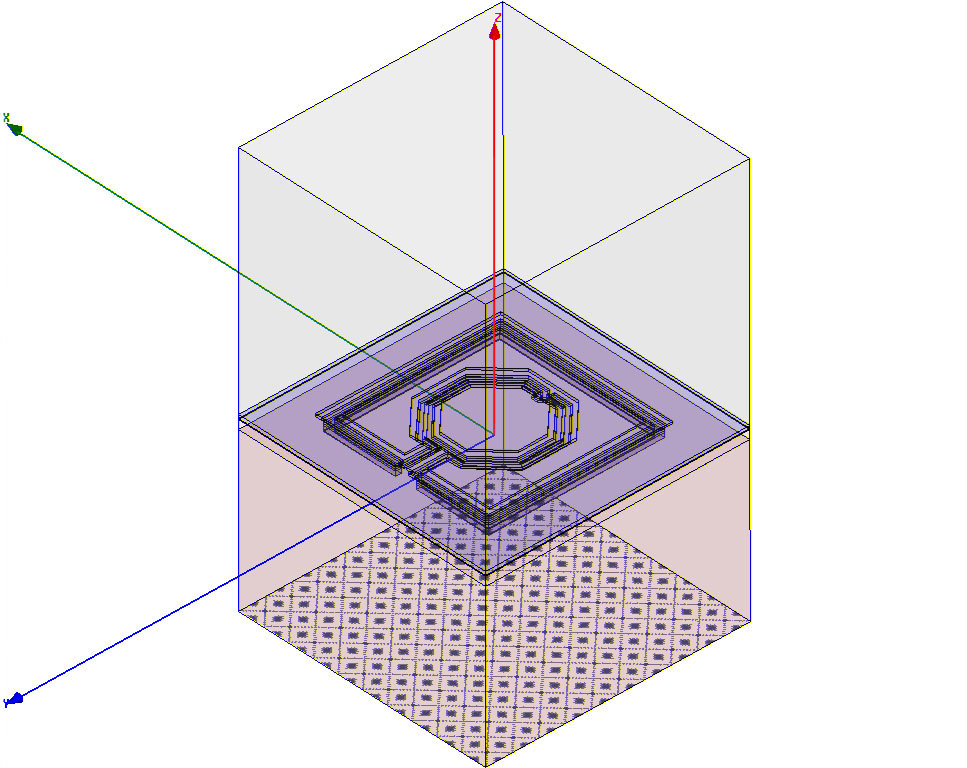
Full 3D EM simulators often don’t have any integration into the layout tools. Hence, rendering the model for simulation requires import of a gds database followed by extensive manual drawing of the component and associated layers not captured in layout such as the substrate, ground planes, passivation, package fill etc. This is both time consuming, very error prone and not conducive to repeated reiteration and optimization of the components impedance. In an ideal flow, the 3D model should be automatically created from the 2D version captured with the layout tool.
We employ a design flow based on industry standard 2D and 3D EM simulators that uses the layout tool as the source to render the model. In this flow, the designer need only handle the layout in the familiar Virtuoso environment. Rendering of the model and subsequent extraction of S-Parameters is done by automatically drawing the 3D model through custom VB or Java script control of the EM simulator given pertinent process specific stack up details and material properties.
For a typical inductor shown in the example below, the layout is done quickly with a custom PCell that includes the ground cage and a choice from all the most commonly used inductor, differential inductor and transformer structures. Once the PCell is placed and sized, the layout is exported to gds. The rest of the process is automated based on custom Java scripts that:
- Start the EM simulator
- Import the model
- Merge common layers
- Add the substrate, oxide, passivation and package fill layers
- Add the ground plane and radiation boundaries
- Add the ports and analysis setup
- Runs the simulation and;
- Exports the S-Parameters to an N-Port file for use in simulations
CAD Support
Analog CAD tools seem to need a patient hand to coax them into submission. Too often designers find themselves changing DRC/LVS decks, scrambling to find alternate simulators, scaling back post layout simulations when extracted netlists grow too large, etc etc. Setup and support of a robust tool flow that enables efficient front to back design with adequate post layout simulation coverage can be laborious. Having had to do this on a daily basis for years, we are well positioned to help with CAD issues arising from most industry standard tools. We are intimately familiar with industry standard tools including Cadence DFII, Virtuoso, Diva and Assura flows, Agilent ADS and RFDE, HSIM, HFSS and others.
Layout & Physical Verification
With most RF IC blocks, even the most carefully designed circuit at the schematic level will only be as good as its implementation in layout. Layout of sensitive blocks takes attention to detail that can only be realized with repeated reiteration of the layout and subsequent re-simulation. Further to this, knowledge of the extraction tools and their limitations is essential to ensure meaningful post layout simulation results.
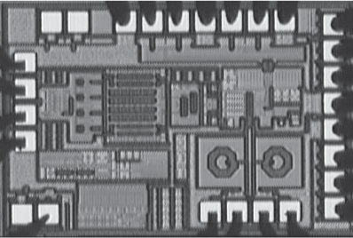
We have extensive experience with sensitive analog layout including image reject mixers, single sideband mixers, frequency scaling circuits and many other designs that require delicate balance of layout parasitics. Not limited to small RF blocks, we have worked primarily with large scale system on chip designs including GSM and 802.11a/b/g transceivers. As an example, the image reject mixer shown in the die photo below acheives an average uncalibrated sideband rejection of 48dB with a 1-sigma standard deviation of 5.7dB measured across the wafer.
We have a wide range of experience with most commonly used foundries as well as setup and management of the Diva and Assura tools in addition to customization of design kits to accommodate anything from a foundry error fix to handling custom components created as part of the design flow. We will become acquainted with your foundries design submission procedures and handle the final physical verification checks and deliver the gds for fab as required.
| HOME | SERVICES | PUBLICATIONS | ABOUT US | CONTACT | DOWNLOADS |