Testing and Verification
Manual Verification
The peak of anxiety in the design cycle, the initial manual rough checks to see if the part works can be time consuming if everything is being exercised for the first time. Serial interface programming may not be timed as expected and just getting the chip powered up and in the correct state sometimes takes some teething. Once manual checks show promise and parameters seem within expectations, it is often prudent to migrate to more automated tests for repeatable and consistent results.
We have never had any circuits we have designed tested first by anyone but ourselves. We have extensive lab experience ranging from artistic soldering jobs to coding up custom baseband signals in the VSG. We are well versed in equipment setup and methodology for running most all required test metrics in RF transceivers and analog blocks.
Test Automation
Even a simple test bench with a small selection of equipment becomes quite versatile when everything is put under GPIB (or TCP/IP) control with some simple scripts. The scripting language can be MATLAB, Python or even a graphical GUI such as VEE. Whether the measurement is something as simple as finding the compression point of an amplifier or doing an exhaustive blocker qualification, when measurements are done manually the likelihood of error increases.
When automated, if a particular setting was found to be in error, then it will have been done the same way for every measurement and can be corrected and repeated with relative ease. We have setup many automated test setups using VEE, Python and more commonly MATLAB. With an inexpensive GPIB and NiDAQ card, one interface can be used to program the DUTs digital interface and then proceed to make the required measurements and process and collect statistics on the results as desired.
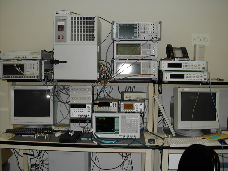
The example below, although not esthetically appealing, shows a recent test bench we setup that runs exhaustive characterization of an 802.11a/b/g RF front end. The program allowed either a detailed characterization of the part (taking approximately 1 hour) or a quick characterization and functionality check (taking approximately 1 minute) to be done. The interface was so simple that anyone could run it without any knowledge of what was being tested. The quick characterization allowed entire batches of thousands of parts to be tested (this is made easier if someone’s kids want to make a couple bucks feeding parts all day) giving immediate insight into yield and most common failure points.
The extended characterization would not proceed unless the basic functionality check passed. The program then gathered receive and transmit:
- Transmit output noise
- Receiver noise figure
- Rx and Tx P1dB and OIP3
- Spurious emissions
- Power consumption
- Synthesizer lock range
- Blocking performance
- Tx and Rx gain flatness and frequency response
- VCO tuning range
- Rx and Tx PGA control range
- Port impedance matching
In addition to other measurements, when completed, a database of data corresponding to each part was available from which a single script could be run to compile detailed statistical results. This was all done over full corners of temperature, supply and I/O common mode levels.
Wafer Probing
Although limited to the testing of small sub cells, wafer probing is an excellent way to verify the individual blocks in a signal chain. It allows a jump start on testing by weeks since the packaging cycle is skipped and is greatly simplified since PCB design and cost are removed. With the right probe station and some automated scripts to control the instruments, probing allows fast testing of large sample sizes across the entire wafer if a dedicated fab run is done. Probing also allows resonant circuit tuning to be easily done with the addition of a laser attachement. This often proves much more effective than having multiple versions of chips fabricated with slightly different tuning.
Once individual blocks in the signal chain are tested via wafer probing, one gains early insight into the performance of the packaged parts that soon follow, giving a heads up to any potential problems that may arise. The caveat to wafer probing is that experiments must be carefully planned out well before tapeout. Unless costly probe frames are used, most stations can only accommodate a couple RF IO GSG or GSSG tips, a couple custom DC wedges and some single needles scattered around the orthogonal probes.
To ensure proper decoupling of the supplies, the DC wedges, and hence the probe pad layout must be planned at the circuit design stage. We have designed and tested many different RF and low frequency analog wafer probing scenarios and can ensure successful probe testing of your designs.
| HOME | SERVICES | PUBLICATIONS | ABOUT US | CONTACT | DOWNLOADS |